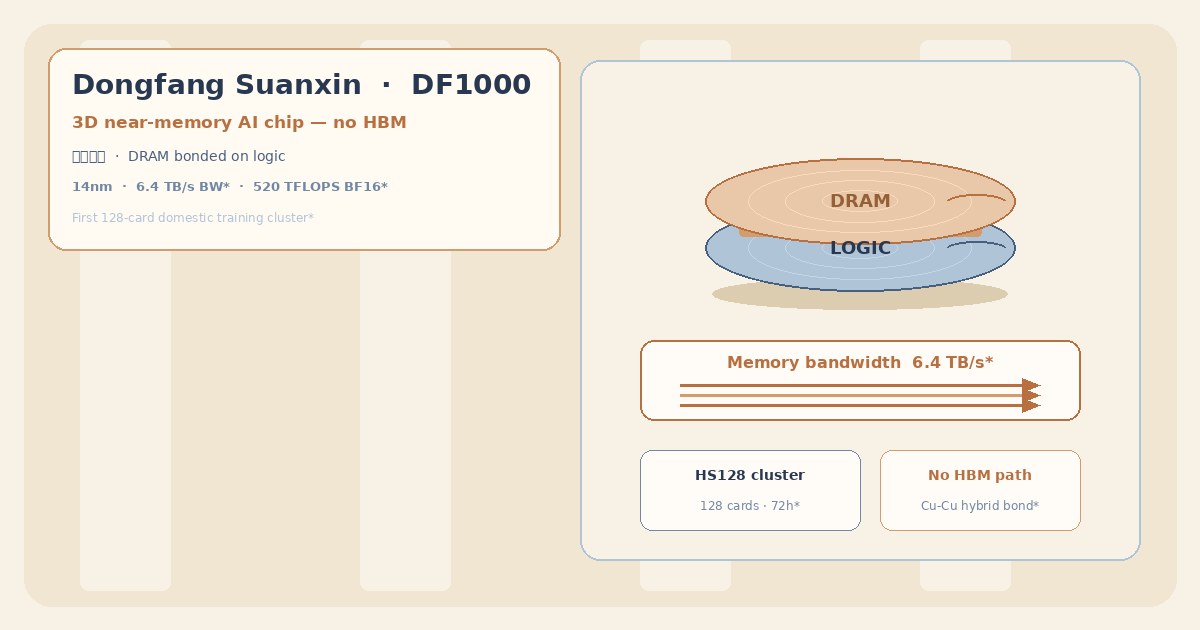
Training clusters have a bandwidth problem as much as a FLOPS problem. HBM is scarce, expensive, and geopolitically concentrated; process nodes below 7nm are constrained for Chinese fabs. DF1000’s bet is a third path between custom ASICs and GPGPU copies: keep logic at a reachable 14nm node, then recover memory bandwidth by stacking DRAM directly on the compute die with wafer-level hybrid bonding. Vendor numbers put peak BF16 compute at 520 TFLOPS*, on-chip memory bandwidth at 6.4 TB/s*, and scale-up interconnect at 900 GB/s*. Whether those envelopes survive silicon and software scrutiny is the open question — but the architectural claim itself is the news for overseas infra teams watching China’s HBM-alternative experiments.
What DF1000 is
Press and company framing call DF1000 a software-defined near-memory 3D AI chip. Mechanically, that means:
- DRAM wafer bonded atop logic wafer — Cu-Cu hybrid bond, no bumps / no interposer in the vendor description*
- 14nm process for the logic side
- BF16 peak 520 TFLOPS*
- Memory bandwidth 6.4 TB/s*
- Scale-up interconnect 900 GB/s*
- Compute efficiency claimed ≥85%* (vendor)
The “software-defined” half is positioning: soft-defined compute plus 3D near-memory as China’s “third path” versus pure ASIC and GPGPU-shaped designs. Three use cases are cited in coverage: LLM training, AFD-style distributed inference, and single-node LLM inference.
Honest answer: no retail SKU, no public cloud listing found, no Digi-Key board, no open weights, nothing overseas labs can buy on Amazon this afternoon. This is architecture + cluster-delivery news from Chinese press (AI123, 至顶科技, 界面新闻, and July securities-journal coverage of the chip launch). Treat it as a supply-chain / HBM-alternative watch item for infra architects — not a purchase order. If a cloud or OEM listing appears later, re-check; as of this writing the deliverable is a delivered domestic cluster story, not an exportable product page.
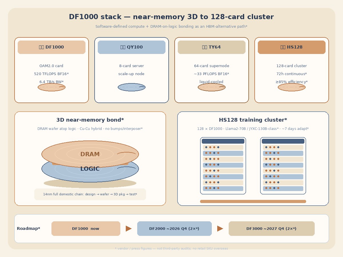
Product ladder 巅峯 DF1000 → 擎元 QY100 → 拓域 TY64 → 慧算 HS128, plus bonded-wafer detail and DF2000/DF3000 roadmap*. Asterisks mark vendor/press figures.
Cluster delivery: 128 cards, 72 hours*
Chinese coverage around the Shanghai 国芯展 says the first domestically fully-sourced large-scale training cluster based on DF1000 has been delivered. The headline configuration is the 慧算 HS128 — 128 DF1000 cards — with claimed continuous training for 72 hours without interrupt*. Workloads named in press include Llama2-70B and JYXC-130B / Step 130B-class ~100B-parameter training tasks*, with model adaptation reportedly taking about 7 days* for a 100B-class model. A thousand-card cluster is framed as planned by end-2026*. None of these are independent audits; they are company and trade-press claims.
Product stack
- 巅峯 DF1000 — OAM2.0 accelerator card (the chip/card SKU)
- 擎元 QY100 — 8-card server
- 拓域 TY64 — liquid-cooled 64-card supernode, ~33 PFLOPS BF16*
- 慧算 HS128 — 128-card cluster (the delivered training system)
Roadmap slides in coverage point to DF2000 ~2026 Q4 (≈2×*) and DF3000 ~2027 Q4 (≈2× again*). Full domestic supply chain is claimed end-to-end: design → 14nm wafer → 3D packaging → test*.
Company and timeline
东方算芯 was founded May 2024 in Shanghai Zhangjiang. CEO/chairman Wei Shaojun (魏少军) brings a well-known Tsinghua / Chinese semiconductor-policy pedigree — relevant context for overseas readers who track which new AI-chip houses have establishment weight behind them. The DF1000 chip was announced July 13, 2026 (界面新闻 and securities-journal coverage); cluster-delivery stories landed at the Shanghai 国芯展 window, with AI123 updating around Oct 30–31, 2026 and 至顶科技 coverage around mid-October.
How this sits next to other ChinaHotTech chip posts
Do not merge DF1000 with earlier ChinaHotTech chip coverage. Rockchip RK1828, XHEART X7 Ultra, Nuclei NI1000, SpacemiT V100, Infenisis Taiyi, Tianmou, StartLux, Amlogic, and similar posts are different product classes — edge/auto SoCs, RISC-V IP, server CPUs, or developer boards. DF1000 is a near-memory training accelerator + domestic cluster delivery story: HBM-alternative packaging and supply-chain completeness, not a hobbyist board or open IP core.
Caveats
- Vendor / press benches* — 520 TFLOPS BF16, 6.4 TB/s, 900 GB/s interconnect, ≥85% efficiency, 72h uptime, ~7-day 100B adapt, TY64 ~33 PFLOPS, DF2000/DF3000 2× claims, and “no bumps/interposer” bonding details all come from company framing and Chinese trade press; not re-measured here.
- No overseas buy path today — not a Digi-Key part, not open weights, not a listed public-cloud instance found for this write-up.
- Young company — founded May 2024; cluster delivery is early-product news, not a multi-year fleet track record.
- 14nm tradeoff — reachable process + packaging bandwidth is the thesis; density and energy vs cutting-edge HBM GPUs remains unproven in third-party benches.
- Distinct from prior chip posts — not RK1828 / XHEART / NI1000 / SpacemiT / Taiyi / Tianmou / StartLux / Amlogic.
Bottom line: DF1000 is Dongfang Suanxin’s public bet that 3D near-memory bonding on 14nm can substitute for scarce HBM in domestic training clusters — and Chinese press now says a 128-card system has been delivered and run for 72 continuous hours*. Overseas engineers should read it as architecture and supply-chain signal, keep asterisks on every number, and not expect a shopping-cart SKU.