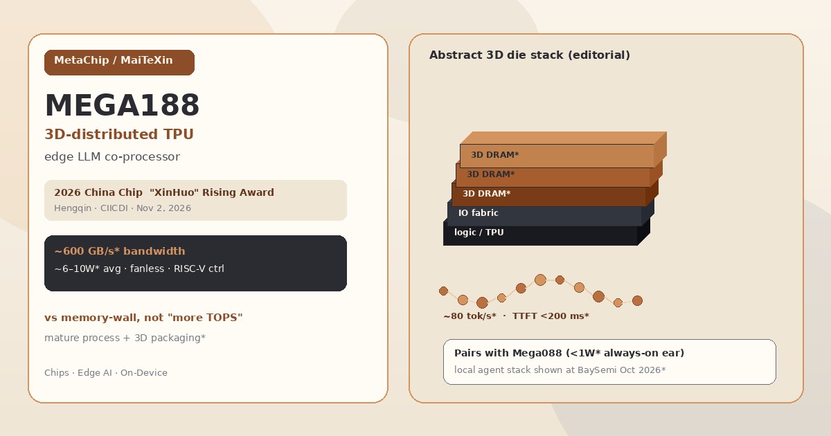
On-device and edge LLM decode is usually bandwidth-bound and power-capped long before the MAC array runs out of math. Phone NPUs and laptop NPUs paper over that with LPDDR channels and aggressive quantization; datacenter GPUs solve it with HBM and a wall socket. MEGA188’s bet — per MetaChip and the award write-ups — is different: 3D DRAM stacking married to distributed AI compute, on a mature domestic process and packaging stack, so the co-processor can sit next to a mainstream host and run open models without a fan. That is why this chip shows up as an architecture-and-supply-chain signal even if you cannot order one from Digi-Key tomorrow.
What the award actually says
爱集微 / 集微网 coverage of the Hengqin ceremony frames MEGA188 as the domestic first for a fully-domestic-process part carrying a self-designed 3D distributed TPU for edge LLM co-processing. The China Chip program (中国电子信息产业发展研究院 / CIICDI) has run twenty-one cycles since 2006; the XinHuo Rising slot is aimed at innovative, high-potential products rather than pure volume champions. MetaChip’s South China systems GM collected the medal. Treat “first” as a press/award claim*, not an independent audit of every prior die — the useful content is the architecture story that won the slot.
Hardware autonomy language in the same pieces is concrete enough to list: national 3D-IC supply chain*, RISC-V control core*, domestic standardized high-speed I/O*, and MetaChip’s own edge LLM toolchain*, with hooks into mainstream host platforms*. That package is the company thesis for why OEMs in embodied AI, smart education, industrial edge, and automotive electronics are early customers* — again, vendor-stated.
Not as a Western cloud SKU and not on Digi-Key. Expect China systems houses and OEM design-ins first. Watch MEGA188 as a packaging-plus-architecture signal on the domestic edge-AI path — distinct from phone NPUs and from datacenter GPU clusters already covered here (Moore Threads / Iluvatar).
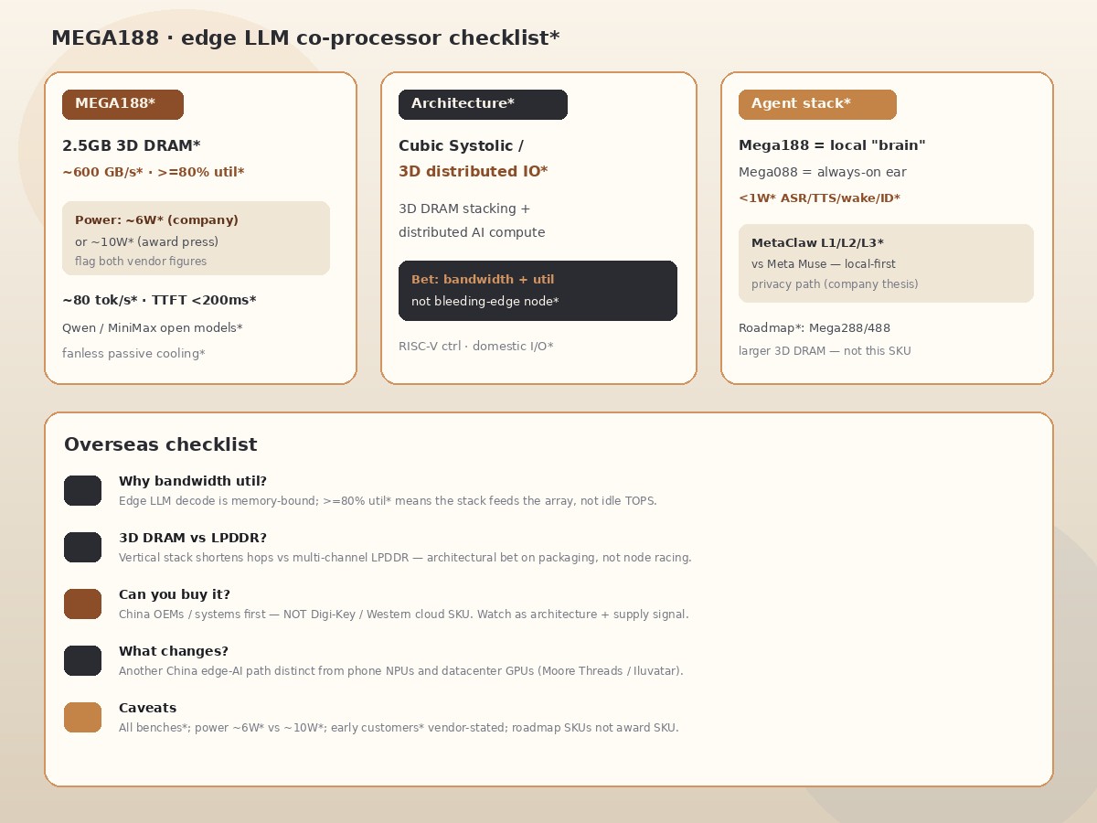
Specs / architecture / agent-stack cards + overseas checklist. Asterisks mark vendor or press figures — not independent China Hot Tech benches.
Numbers worth keeping — all asterisked
Press and company pages do not always say the same wattage, so flag both. Award / 爱集微 copy cites full-chip average power around ~10W*; MetaChip / BaySemi (湾芯展) product framing cites around ~6W*. Bandwidth is consistently quoted near ~600 GB/s*, with company materials adding 2.5GB 3D DRAM* and ≥80% bandwidth utilization*. Inference marketing for open models (Qwen / MiniMax 面壁 and peers*) lands at roughly ~80 tok/s* peak with TTFT under 200 ms*, under fanless passive cooling*. Those are the numbers to pressure-test if a board ever lands on your bench — do not flatten the 6W/10W split into a single unasterisked figure.
Why utilization matters: peak bandwidth is a ceiling; decode tokens starve when the stack cannot keep the array fed. A claimed ≥80% util* is MetaChip arguing the 3D path actually moves data, not that the die merely advertises a wide bus. Why stacking versus more LPDDR channels: vertical DRAM-on-logic shortens physical hops and can raise effective bandwidth per watt without chasing the newest logic node. That is the “mature process + 3D packaging instead of bleeding-edge nodes”* thesis company roadmap pieces lean on — an engineering trade, not a morality play about process leadership.
Architecture sketch (vendor naming)
Company materials describe a Cubic Systolic / 3D distributed IO style fabric: 3D DRAM layers stacked with distributed AI compute so the co-processor behaves as a local “brain” for agent workloads rather than a classic vision NPU bolted onto a SoC. A RISC-V control core and domestic high-speed I/O are the host-facing glue. The useful mental model for overseas readers is co-processor + host, not a phone AP replacement and not a rack GPU. If your mental map only has “NPUs inside phones” and “GPUs in clouds,” this is the third lane China edge vendors keep trying to pave.
Mega088, MetaClaw, and the personal-agent stack
At 湾芯展 (BaySemi) on Oct 14, 2026, MetaChip showed MEGA188 paired with Mega088 as a “personal agent” stack: Mega088 as the always-on ear (ASR / TTS / wake / voice ID at under ~1W* full load*), Mega188 as the intermittent brain for heavier local LLM turns. The company frames this under MetaClaw / 个人智能体 with L1 / L2 / L3 layers, positioned as a local-first privacy path versus Meta’s Muse-style on-device narrative. Treat the Muse comparison as marketing contrast*, not a side-by-side product review — the engineering takeaway is the split between always-on microwatt-class voice silicon and a fanless ~single-digit-watt LLM co-processor.
Roadmap slides mention Mega288 / Mega488 with larger 3D DRAM for bigger models*. Mention them only as roadmap*; do not confuse them with the MEGA188 award SKU that actually collected the XinHuo medal.
Caveats
- Vendor benches* — tok/s, TTFT, bandwidth util, model list, and early-customer verticals come from MetaChip / award press; no independent China Hot Tech lab numbers.
- Power split* — ~6W* (company / BaySemi) vs ~10W* (award article); report both until a datasheet settles it.
- “First” claim* — award/press language; useful as positioning, not as a litigation-grade exclusivity proof.
- Not Digi-Key / not a Western cloud SKU — China OEM and systems path; availability outside that channel is unclear.
- Roadmap ≠ award SKU — Mega288/488 are larger-DRAM follow-ons*; MEGA188 is the part that won XinHuo.
Bottom line: MEGA188 is MetaChip arguing that edge LLM inference is a packaging-and-bandwidth problem, and that a domestic 3D DRAM + distributed TPU co-processor can sit in the personal-agent stack next to a sub-watt always-on ear. Overseas engineers should read it as another China edge-AI path — distinct from phone NPUs and from the datacenter GPU halls — and keep every asterisked number in the vendor column until boards and datasheets circulate.