

Wearable GUIs have spent the last few years asking more of a very small budget: vector watch faces, health and fitness traces, navigation polylines, and the rings and gauges that show up on a round display, all drawn under tight power and on-chip SRAM limits. VeriSilicon’s answer, dated November 5, 2026 on both its English and Chinese press pages (the same text went out on PR Newswire and was reprinted by 集微网 / Jiwei), is not a new application processor. It is a next-generation 2.5D GPU IP named GCNanoOptimaV, built for that wearable socket and described as already adopted by multiple leading customers*. Those customers are not named, and the note publishes no performance, power, area, process-node, or SRAM-kilobyte figures — so none are invented here.
If you already know Vivante’s 2.5D line, VGLite, or LVGL on a watch or band MCU, the pitch is specific: take the strokes, curves, and ellipses that dominate those screens out of a general-purpose path and put them in dedicated hardware, then change how meshes are rendered so the block asks for less on-chip SRAM*. Compatibility with the existing VGLite API, plus LVGL, SVG, and PNG*, is how the vendor says you move an existing UI over with minimal modifications*.
What the note actually specifies
GCNanoOptimaV is described as featuring dedicated hardware acceleration engines and an optimized memory architecture*, so it can deliver richer and more responsive graphical user interfaces while staying inside wearable resource limits*. The two engines the company names are a Hardware Stroke Engine and a Hardware Ellipse Engine*, aimed at well-known bottlenecks in vector graphics. The stroke engine is said to improve rendering of complex lines and curves, “particularly in applications such as health monitoring, fitness tracking, and navigation”* — in other words, the traces, routes, and map polylines that a watch draws over and over. The ellipse engine is listed alongside it in the same sentence of the official note; VeriSilicon does not publish a separate benchmark for arcs, rings, or circular gauges, so treat that as an architectural claim rather than a measured frame-time delta.
Memory is the other half of the announcement. An “innovative mesh rendering architecture” is said to reduce on-chip SRAM requirements*, which would matter in an SoC that already spends a large share of its SRAM on framebuffers and UI working sets. The company does not publish a percentage, a kilobyte figure, or a before-and-after buffer size, and we are not going to invent one. GCNanoOptimaV also integrates VeriSilicon’s latest DECNano 3.0 compression engine, which the vendor says delivers improved image quality while maintaining a fixed 2:1 compression ratio*. A fixed ratio is at least a number an SoC architect can plan around: whatever quality claim you attach to 3.0 versus the previous DECNano generation, the compression ratio itself does not float with content.
On the software side, the GPU “maintains compatibility with VeriSilicon’s VGLite graphics API” and “supports widely adopted graphics frameworks and formats, including LVGL, SVG, and PNG”*. That compatibility, the note says, “facilitates the migration of existing applications with minimal modifications”*. If your wearable UI is already on VGLite or talking to this vendor’s SVG path (VeriSilicon has previously pointed at its open-source SvgVGLiteRenderer in older 2.5D materials), the intended upgrade is a drop-in IP swap rather than a rewrite. The launch note does not describe a new programming model.
Licensable GPU IP — not a chip on Digi-Key or Mouser. You integrate GCNanoOptimaV into an SoC (or ask your foundry / ASIC partner to), then bring up VGLite and your LVGL or SVG UI on top. Inquire through the company site and sales offices at verisilicon.com; there is also an “Ask for Details” link on the Vivante 2.5D GPU family page. The address [email protected] is the media contact printed on the press note, not a sales inbox. The vendor says multiple leading customers have already adopted the IP*; it names none of them, and it publishes no pricing, license terms, process-node ports, or evaluation-kit schedule. Do not plan a tape-out around an availability date that was never given. Every performance, power, SRAM, and “already adopted” claim below is a vendor statement until you see a datasheet and measure the block in your own process and memory map.
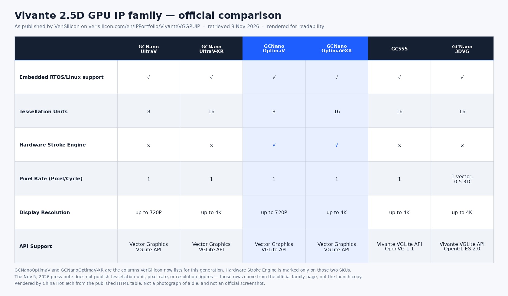
Not a photograph of a die. A readability rendering of the comparison table VeriSilicon publishes on its official Vivante 2.5D GPU IP page (retrieved November 9, 2026), which now includes GCNanoOptimaV and GCNanoOptimaV-XR as their own columns. Hardware Stroke Engine is marked only on those two SKUs. The November 5 press note itself does not list tessellation-unit, pixel-rate, or resolution figures — those rows come from this family page, not from the launch copy.
What the official family page adds
The launch note is qualitative. The product-family page is slightly less so. On verisilicon.com/en/IPPortfolio/VivanteVGGPUIP, VeriSilicon now lists GCNanoOptimaV next to GCNanoUltraV, the XR variants, GC555, and GCNano3DVG. For GCNanoOptimaV the published cells are: embedded RTOS/Linux support; 8 tessellation units; Hardware Stroke Engine: yes; 1 pixel/cycle; display resolution up to 720P; and the Vector Graphics VGLite API. A sibling column, GCNanoOptimaV-XR, shares the stroke engine and the 1 pixel/cycle rate but lists 16 tessellation units and display resolution up to 4K. The November 5 press release announces “GCNanoOptimaV” and does not mention the XR SKU by name; the XR row is included here only because it appears on that official family table.
Two cautions follow from reading the table next to the press note. First, “up to 720P” for the base OptimaV part is a family-page spec, not a sentence in the wearable launch copy — cite the product page if you use it in a checklist, and do not promote it into a “720p watch panel” marketing line the company did not write. Second, the family table has a Hardware Stroke Engine row (the clear differentiator versus GCNanoUltraV, UltraV-XR, GC555, and GCNano3DVG, all marked no) but no Hardware Ellipse Engine row. The ellipse engine exists in the press note; it is not broken out as its own comparison cell. Pixel rate and tessellation-unit counts are likewise family-page figures, not launch-note figures. Older Vivante/GCNano datasheet numbers — gate counts, SRAM sizes, process nodes, frame rates, milliwatts — are not automatically OptimaV numbers, and this launch did not refresh them.
The quote, and what it does not quantify
Weijin Dai, Chief Strategy Officer, Executive Vice President, and General Manager of the IP Division, is quoted in the official note: wearable devices are evolving rapidly, “with increasingly sophisticated applications driving demand for greater functionality and higher graphics performance, while power consumption and memory footprint remain critical constraints.” Through architectural innovations and advanced hardware acceleration, he says, “our next-generation 2.5D GPU IP delivers measurable performance improvements and power savings in applications such as mapping and navigation,” enabling richer visual experiences inside those power and memory budgets*.
“Measurable” is doing a lot of work in that sentence. No frames-per-second, no milliwatts, no percentage speedup, and no millijoules-per-frame appear in the English note, the Chinese note, or the PR Newswire pickup. Mapping and navigation are named as the example workload, which lines up with the stroke-engine story, but you cannot size a power rail or an SRAM compiler from this announcement. If you are comparing the block against another ultra-low-power vector GPU, you will need an evaluation deliverable the company has not put on the public page.
Where this sits in the existing 2.5D line
VeriSilicon’s Vivante 2.5D GPU series is pitched at MCU and MPU designs that want hardware-accelerated UI — smart watches, bracelets, navigators, automotive, and other embedded screens — on top of the company’s ScalarMorphic architecture, according to the same family page. That is context for the line, not a spec dump for OptimaV. The previous publicly discussed member, GCNanoUltraV, already carried VGLite, LVGL, and SVG; what this generation adds in public is the dedicated stroke (and, in the press note, ellipse) hardware plus the mesh-rendering / SRAM claim* and DECNano 3.0*.
Earlier official design-ins on that older generation are worth keeping separate from this launch’s unnamed customers. In November 2023 VeriSilicon said LG Electronics selected GCNanoUltraV for a next in-house SoC*. In May 2024 it said Actions Technology adopted its 2.5D GPU IP in the ATS3085S and ATS3089 dual-mode Bluetooth smart-watch SoC series, with those watch products described as already in mass production*. Those are previous-generation / family design-ins, documented on VeriSilicon’s own press pages. They are not named GCNanoOptimaV customers, and we are not treating them as such.
This is also not a sequel to Coral. On October 22 we wrote about VeriSilicon’s path around Google’s open Coral NPU — edge AI acceleration, not display. GCNanoOptimaV is a 2.5D GPU for drawing the UI that a wearable already has to refresh all day. Different IP category, different integration question, different evaluation checklist.
Who the vendor is
VeriSilicon Microelectronics (Shanghai) Co., Ltd. (芯原, 688521.SH) is a publicly listed custom-silicon and semiconductor-IP company founded in 2001 and headquartered in Shanghai. The “About VeriSilicon” blurb attached to this press note says it has 9 design and R&D centers and 10 sales and customer service offices worldwide and employs more than 2,000 people. Its stated model is Silicon Platform as a Service (SiPaaS): license internally developed processing IP — GPU, NPU, VPU, DSP, ISP, and display-processing, plus a large analog / mixed-signal catalog — and use those blocks as the basis for custom ASICs and platforms. The customers listed in that blurb are fabless companies, IDMs, OEM/ODM system vendors, large internet companies, and cloud providers. For an overseas SoC or wearable-firmware team, the practical path is a license conversation with VeriSilicon or with an SoC vendor that already takes this IP, not a reel of parts from a catalog distributor.
What changes (and what does not)
- A new 2.5D GPU IP for wearables, not a chip — GCNanoOptimaV is licensable semiconductor IP. You cannot buy it on Digi-Key; you license it into an SoC.
- Hardware Stroke Engine + Hardware Ellipse Engine* — dedicated paths for complex lines, curves, and ellipses, with health monitoring, fitness tracking, and navigation called out as the stroke-engine examples*. No public frame-time or milliwatt numbers.
- Mesh rendering said to cut on-chip SRAM* — qualitative only; no percentage or kilobyte savings were published.
- DECNano 3.0 at a fixed 2:1 compression ratio* — the ratio is the one hard number in the launch note; the “improved image quality*” claim is not quantified.
- VGLite compatibility, plus LVGL, SVG, and PNG* — vendor says existing applications migrate with minimal modifications*.
- Family-page cells for OptimaV (not in the press note): 8 tessellation units, 1 pixel/cycle, display resolution up to 720P, Hardware Stroke Engine marked yes, VGLite API — from the official Vivante 2.5D table. OptimaV-XR is listed there with 16 tessellation units and up to 4K; the launch PR does not name the XR SKU.
- Already adopted by multiple leading customers* — unnamed. Do not assume last-generation UltraV licensees (LG in 2023*, Actions ATS3085S / ATS3089 in 2024*) are OptimaV design-ins.
- No public PPA, process node, gate count, SRAM map, or sample calendar — Dai’s “measurable performance improvements and power savings… in mapping and navigation*” remains unmeasured in public.
Bottom line: if you already license Vivante 2.5D GPU IP, or you ship a wearable UI on VGLite and LVGL, GCNanoOptimaV is the first public signal that VeriSilicon wants the expensive vector work — strokes, ellipses, and the SRAM those paths consume — moved into dedicated hardware without breaking the API you already wrote to. Keep every performance, power, SRAM, quality, and “already adopted” claim asterisked, wait for a datasheet that actually quotes PPA, and do not confuse this GPU IP with the Coral NPU story or with a chip you can order by part number tonight.