If you work on industrial HMI, multi-axis motion, or a robot joint that has to talk EtherCAT in a very small hole, GigaDevice already had parts in this family. The English note dated November 10, 2026, and datelined Munich — also carried on Business Wire — does not quietly invent a new silicon family. It gathers three already-announced cuts under one “full-scenario industrial” story, timed to electronica (November 10–13, official graphic: hall booth C5.221*), and it prints a new sample and production calendar that a Western program can actually put on a spreadsheet.
This is also not the GigaDevice part we wrote about yesterday. The GD32F50MxxG is a 252 MHz Cortex-M33 that co-packages a three-phase gate driver for 24–48 V FOC joints. GD32H7 is a high-end Cortex-M7 industrial line. Same vendor, different socket. Do not treat a Munich portfolio note as a replacement for that driver-in-package chip, or the other way around.
What was already announced, and what November 10 actually changes
The company’s own Chinese newsroom is the cleanest timeline, and it does not match a “brand-new MCU today” headline:
- December 18, 2025 — GD32H78D / H77D, the HMI-leaning cut: 750 / 600 MHz* M7, a 2-lane MIPI DSI*, an image-processing accelerator*, and 2 MB execution Flash + 8 MB storage Flash* with 1.2 MB SRAM* and 640 KB TCM*. BGA176*. Mass production was then aimed at June 2026*. That same note is also the source of the family’s often-quoted 3,736 CoreMark* / 4.98 CoreMark/MHz* figure, which is a 750 MHz number, not a 600 MHz one.
- January 22, 2026 — GD32H78E / H77E (EtherCAT slave* for real-time motion) and GD32H789 / H779 (general-purpose industrial). Same 750 MHz* ceiling, same 2 MB + 8 MB Flash* and 640 KB TCM* story. Mass production was again aimed at June 2026*.
- August 5, 2026 — GD32H77R, the robot-joint / servo cut: 600 MHz* M7 in a 9×9 mm BGA169*, with an on-die EtherCAT slave* and two 100 Mbps Ethernet PHYs*. That is the part a joint-module designer should actually ask about.
What November 10 adds is packaging, not a new tape-out announcement. The family is described as coming from a “homologous silicon die” with IP and peripherals tuned per scenario, a shared toolchain, and a shared TÜV Rheinland IEC 61508 SC3 (SIL 2 / SIL 3)* functional-safety package — claims that also appeared, in slightly different wording, in the earlier Chinese notes. The practical change is the calendar. The Munich note says customers can apply for samples through a local sales representative, with full sample availability targeted for January 2027* and mass production scheduled for April 2027*. It does not say which SKUs missed the June 2026 dates, whether some June units already shipped, or whether January/April applies only to later cuts. We are not inventing a reconciliation. If you are quoting a date, ask which orderable part number it belongs to.
One number in the Munich copy should not be copied onto every SKU. The release says the “entire portfolio adopts unified storage specifications, including 2 MB high-speed executable Flash, 8 MB large-capacity storage Flash and 1.2 MB high-speed SRAM.” That 8 MB storage figure matches the December and January notes for the HMI and automation cuts. It does not match the official GD32H77R materials. Treat Flash as SKU-specific until a datasheet says otherwise.
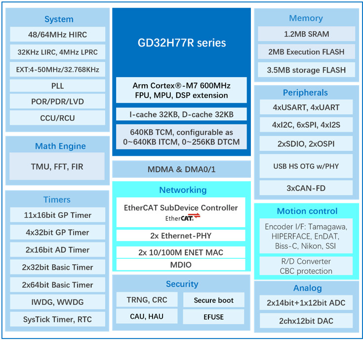
Official “GD32H77R series” block diagram from GigaDevice’s August 5, 2026 Chinese announcement (image dated August 7 on that site). Vendor architecture art, not a die photograph. This is the drawing to use if you are talking about the joint MCU, not the November family prose.
What the H77R diagram actually lists
The August diagram is more specific than the Munich press copy, and it is consistent with the live GD32H77R product page, which currently lists a single orderable string we could see: GD32H77RAPK7, BGA169, 600 MHz, 5632K of on-die Flash. 2,048 KB + 3,584 KB is 5,632 KB — that is the 2 MB execution + 3.5 MB storage Flash drawn on the block diagram, not 8 MB.
On that same drawing, the compute side is an Arm Cortex-M7 at 600 MHz* with FPU, MPU, and DSP extensions, 32 KB I-cache + 32 KB D-cache*, and 640 KB TCM* that the diagram says can be configured as 0–640 KB ITCM and 0–256 KB DTCM*. Next to it sit 1.2 MB SRAM* and a math engine labeled TMU, FFT, and FIR* — the trigonometric / filter offload the Munich note describes as a family feature. Do not hang the 3,736 CoreMark* figure on this 600 MHz part unless a later datasheet says so; that number arrived with the 750 MHz H78D note.
The networking block is why a joint-board designer would care. The diagram labels an EtherCAT SubDevice Controller*, two Ethernet PHYs*, two 10/100M ENET MACs*, and MDIO*. The August write-up says that on-die PHY pair is meant to drop two external industrial PHYs from the BOM, that one-way EtherCAT latency can be “as low as under 50 ns”*, that DC synchronization can reach 62.5 μs*, and that FSoE* is supported against an IEC 61508 SIL 3* claim. Those are vendor numbers. The Munich note repeats the under-50 ns and FSoE claims for the H7xR cut. A 9×9 mm BGA169 with two PHYs on the die is a real board-area argument if the silicon and the magnetics plan work as advertised; it is not, by itself, a drop-in for a Texas Instruments, Renesas, or Infineon EtherCAT node you already have qualified.
Motion peripherals on the diagram are also a bit richer than the August prose. The drawing lists encoder interfaces for Tamagawa, HIPERFACE, EnDAT, Biss-C, and Nikon*, plus an R/D converter* and CBC protection*. The August article named EnDat, BiSS-C, and Tamagawa, and a built-in resolver-to-digital module, but not HIPERFACE or Nikon in that paragraph. The January automation-cut note is the one that added HIPERFACE DSL in prose. If you need a specific encoder protocol, ask for the pin and software support on GD32H77RAPK7, not a family slogan.
The rest of the drawing is a dense but ordinary high-end M7 checklist: 4× USART + 4× UART, 4× I²C, 6× SPI, 4× I²S, 2× SDIO, 2× OSPI, USB HS OTG with PHY, 3× CAN-FD; analog as 2× 14-bit + 1× 12-bit ADC and 2-channel 12-bit DAC; a large timer set; security blocks labeled TRNG, CRC, secure boot, CAU, HAU, and EFUSE*. The August note adds hardware encryption and a CRA / IEC 62443-flavored software story, and says the STL has a TÜV Rheinland IEC 61508 SC3 (SIL 2 / SIL 3) certificate plus ISO 60730 Class B*. Certificates are documents you request, not a caption.
The other two cuts, in brief
If your board is a panel, not a joint, the Munich note points at GD32H78D / H77D (750 / 600 MHz*): 2-lane MIPI DSI* claimed to drive QCIF through XVGA, an IPA* graphics block, compatibility language for LVGL, emWin, Embedded Wizard, and ThreadX GUIX, plus 4× SAI, 4× I²S, and S/PDIF*. That is the December 2025 HMI pitch, restated. If your board is a drive, gateway, or general industrial controller, it points at H7xE (EtherCAT slave*, 62.5 μs DC-sync* in the Munich text, encoder / resolver language) and H7x9 (a 14-bit ADC* and HPDF* digital filter in the same note). Shared family claims also include dual OSPI at 200 MHz DTR*, dual 10/100 Ethernet and 3× CAN-FD*, USB HS/FS and SDIO*, and a 1.71–3.6 V* rail. The August H77R article said 1.7–3.6 V*. Use the datasheet.
Not from a Western catalog click we could find — the published path is a local sales representative, with full samples aimed at January 2027. On November 10, 2026, we did not find a Digi-Key or Mouser catalog product page for GD32H77R or GD32H78D that we could use. An older sibling, GD32H75E, already has a Mouser presence; that is not this portfolio. The company points applicants at its sales network and, on the English product pages, at the GD32H77R page (SKU GD32H77RAPK7) and the GD32H7xx series page. It also promises evaluation boards, FOC motor examples, joint-drive and GUI kits, and the functional-safety package. No public unit price, MOQ, or exact sample week appears in the materials we retrieved, and we are not inventing any. If you are already in Munich this week, the official invitation graphic says booth C5.221, November 10–13, Am Messesee 2. A booth demo is not a packing list.
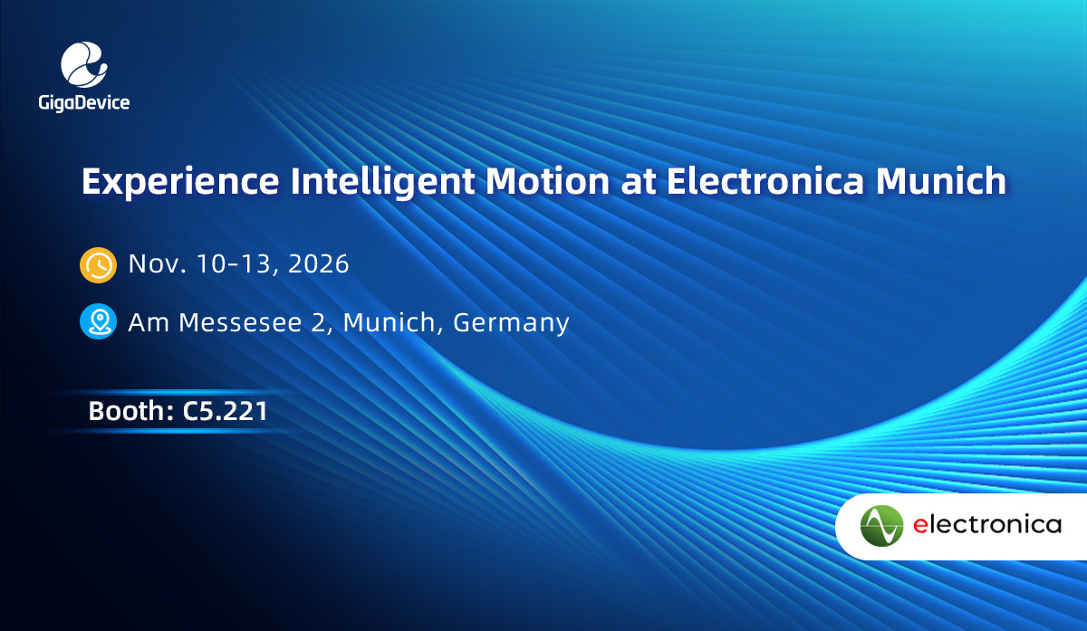
Official GigaDevice invitation graphic from the company’s site (image dated November 9, 2026): electronica Munich, November 10–13, Am Messesee 2, booth C5.221. Event marketing art, not a photo of the booth or of silicon.
What changes (and what does not)
What changes, if you are specifying a 2027 industrial or robot-joint board, is that a Chinese M7 family with a documented joint SKU — on-die EtherCAT plus two PHYs in 9×9 mm, a published 5632K Flash map, and a TÜV-shaped safety package — now has a Munich-facing calendar you can take to a sales engineer this week. For a team already on GD32, or a European machine builder walking hall C, that is a reason to request the GD32H77RAPK7 datasheet, the FMEDA, and a statement of which Flash and which PHY magnetics that orderable part actually has. The “one die, three cuts, one toolchain” pitch is also the company’s answer to having to qualify a different MCU at every node of a cell.
What does not change is the homework, and the history. This is not a November surprise die, and it is not a documented drop-in for the EtherCAT or HMI parts you already have on a cart. The 8 MB “unified” Flash line in the Munich copy does not match the official H77R diagram. The 3,736 CoreMark* figure is a 750 MHz claim. The June 2026 mass-production targets from December and January have been replaced, in public, by January / April 2027, without an explanation of what shipped in between. There is no Digi-Key page we could use. Get the PDF for the exact SKU, ask which calendar applies to that SKU, and treat on-die PHYs, sub-50 ns latency, FSoE, and SIL 3 as claims to check against a datasheet and a certificate — then decide whether this joint MCU belongs on the board.