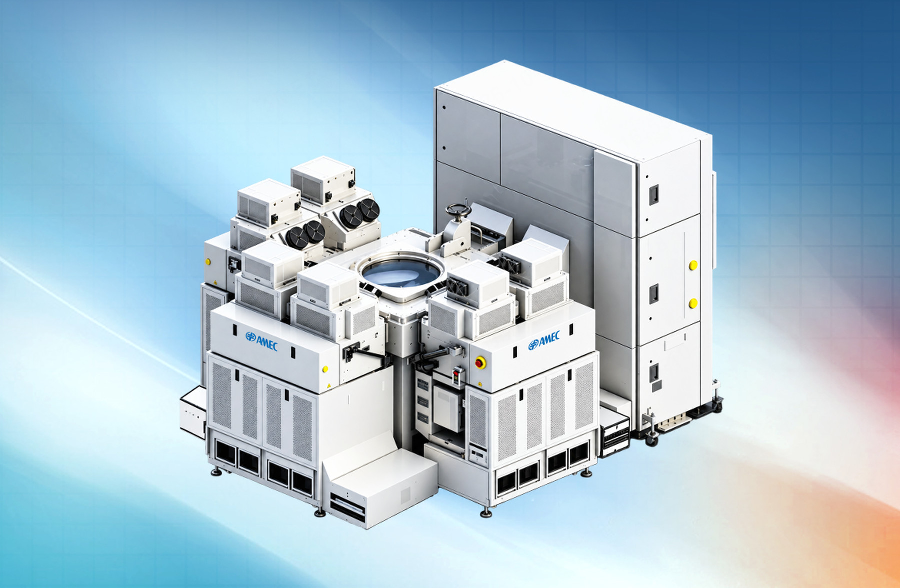
Wafer dicing is the unglamorous step that decides how much of a finished wafer you actually get to package. Blade saws are still the default. They also eat street width, leave chipping risk on thinned or bumped wafers, and get awkward once a packaging flow wants streets measured in a few microns rather than tens. Plasma dicing — etching the streets instead of sawing them — is not a new idea. Panasonic, DISCO, and others have sold tools in that category for years. What is new, as of AMEC’s November 10 post, is that a Chinese etch vendor already present on international lines says it has built its own plasma dicer and has put the first one on a truck.
The primary source is AMEC’s own news page, dated November 10, titled “重要突破!中微公司首台等离子体晶圆切割设备成功交付.” SEMI’s China site, 集邦化合物半导体 via 电子工程专辑, and 新华财经 carried the same note. Treat the street-width, thickness, station-count, and “low cost / high throughput” language as vendor claims until a customer publishes a process-of-record, a wafer-per-hour number, and a yield comparison against the plasma or laser-groove flow they already run. A first shipment is not a qualified tool.
What AMEC is actually claiming
The useful sentence in the official post is the heritage claim, not the adjectives. Primo Matrix, AMEC says, uses the plasma deep-silicon etch already “fully proven in volume production” on Primo TSV, and packages it as a dicing platform with a dual-station etch chamber plus a wafer-transfer module*. In other words, this is an etch company walking its TSV chemistry sideways into singulation, not a startup inventing a new plasma from a slide. The numbers AMEC is willing to put on the new tool, as the official page states them:
- Framed 200 mm and 300 mm wafers, with 300 mm as the main platform and 200 mm as backward compatibility*. That “with frame” wording matters: plasma dicers in packaging often have to handle tape-frame wafers after thinning, not bare front-end wafers.
- Dicing streets “down to 5 μm” at the narrow end, with the usual pitch that a narrower street returns more die per wafer*. Five microns is an aggressive figure next to a mechanical blade. It is also a capability claim, not a published process window, and the post does not say on which stack, mask, or thickness that 5 μm was demonstrated.
- Wafer thickness 25–700 μm*, covering ultra-thin wafers after backside grind as well as more ordinary thicknesses. The post explicitly names post-thinning dicing as a target.
- A system built on the existing Primo platform that “can be fitted with up to six etch stations” for long process times*. The base configuration described in the same paragraph is a dual-station chamber. Do not read “six stations” as the first unit’s as-shipped layout; read it as a platform ceiling.
- Process modes listed by name: front-side plasma dicing of bumped wafers, plasma dicing after laser grooving, and wafer backside etch*, plus a dielectric / hard-mask open etch for wafers with a dielectric layer or a complicated surface*. That is a process menu, not a cookbook.
Two things the official post does not give you: a wafer-per-hour number, and the name of the packaging customer. “Domestic important IC packaging customer” is as specific as it gets. There is also no public list price, no cleanroom footprint, no cost-of-ownership model, and no side-by-side against a Panasonic plasma dicer or a DISCO laser-groove-plus-break flow. Until those exist, the honest status is a first article shipped, with a process menu that looks like the one a packaging engineer would ask for.
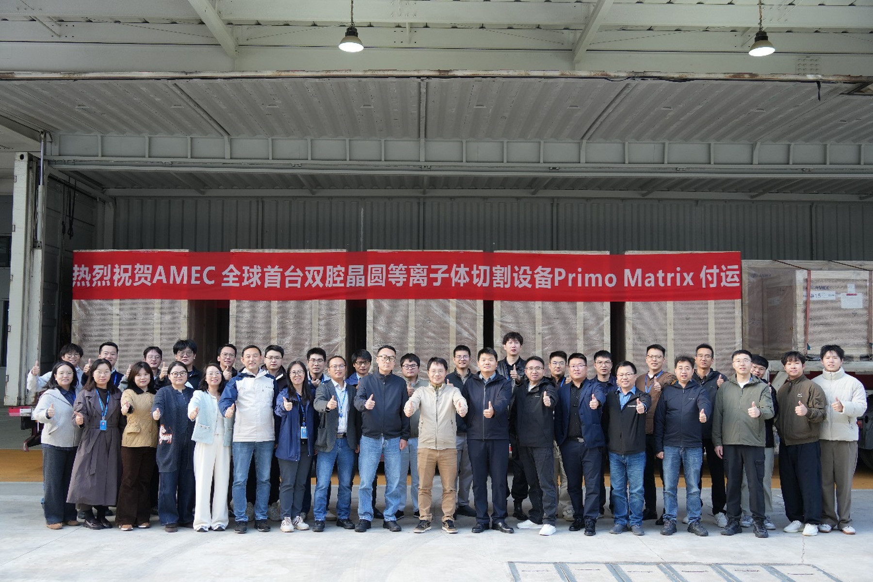
Official AMEC photograph from the same November 10 news post (higher-resolution reprint by 央广网, credited to AMEC): the first-unit shipment ceremony. The red banner congratulates the “全球首台” dual-chamber Primo Matrix plasma dicer on its way out the door. Read that as AMEC celebrating its first unit of this model — plasma dicing as a process, and dual-station plasma tools in general, already exist. The crates are real; they are not a picture of the tool already running in a customer bay.
Do not mix the etch-fleet numbers into the dicer
The same official post spends several paragraphs on AMEC’s existing etch and thin-film business. Those figures are about the company, not about Primo Matrix. As of the end of September 2026, AMEC says it has shipped more than 9,300 reaction stations onto more than 220 production lines at home and abroad, and has developed 54 high-end tool types — 26 etch variants and 24 thin-film tools, plus CMP and packaging / inspection gear*. Its etch coverage claim is 65 nm down to 3 nm and below*. The aspect-ratio numbers in the same paragraph — dielectric etch at 60:1 and 90:1, silicon etch at 140:1, dual-station ICP “at the 0.2 nm single-atom level”* — are etch-fleet marketing, not dicing-street measurements. Do not paste them into a Primo Matrix comparison table.
The five-year ambition is equally easy to over-read. AMEC says it plans, through “organic growth and external expansion,” to cover more than 60% of the high-end semiconductor-equipment market and more than 70% of the advanced-packaging equipment market*. That is a corporate target, not a 2026 share figure, and it is certainly not a statement that one shipped dicer has done either of those things. The product-family chart published with the post is the more useful picture: Primo Matrix is drawn in the “advanced packaging equipment” row, next to other Primo TSV and packaging-oriented tools, as a new member of a large existing catalog.
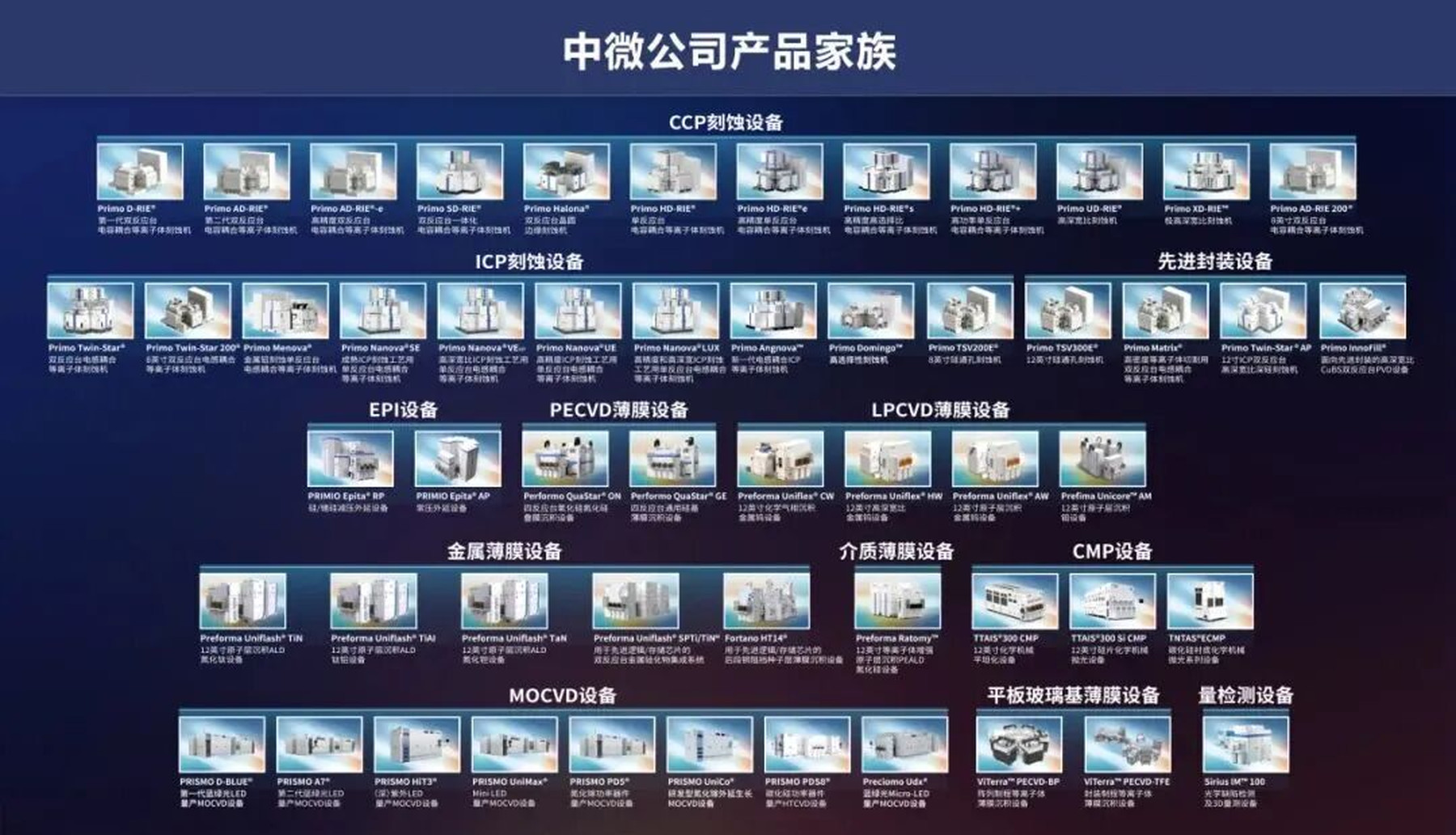
Official AMEC “产品家族” chart from the November 10 news post. Primo Matrix sits in the advanced-packaging row, not in the front-end etch rows. This is a company graphic of the catalog, not a photograph of a installed base of dicers.
Not as a catalog SKU, and not tomorrow on a Western OSAT floor that we can point to. AMEC is a Shanghai-listed tool vendor (688012.SH) with a public international network — including pages for North America, Korea, and Taiwan — and, by its own account, etch tools already running at “domestic and international first-tier customers.” That is a real inquiry path if you already buy AMEC etch, or if you are a packaging house looking at a China-sited plasma-dicing option. It is not the same as ordering a qualified Primo Matrix cell with a published recipe. The first unit went to an unnamed domestic packaging customer. Ask for the as-shipped station count, the 5 μm street demonstration stack, the framed-wafer handling details, throughput, chipping and die-strength data versus the incumbent saw or laser-groove flow, and whether AMEC will support the tool outside China. Then decide whether this is a second-source conversation you want to start, or a press-cycle first article you can watch from the sideline.
What this changes, and what it does not
It does not make plasma dicing a Chinese invention, and it does not retire the Panasonic and DISCO tools already on packaging lines. The process category is established. A shipment ceremony in front of crates also does not tell you uptime, particles, cost per wafer, or whether the 5 μm street survives a real bumped, thinned product wafer at volume. The “全球首台” wording on AMEC’s own banner is celebration of the first Matrix unit; it is not a reason to write “the world’s first plasma dicer.”
What it does change is a narrower question. If you already take AMEC seriously as an etch supplier — because of a China-sited line, because of a second source next to an incumbent, or because you already have Primo TSV process knowledge in-house — is there now a plasma-dicing platform from the same vendor, with a process menu that names bumped wafers, laser-groove-then-plasma, and backside etch, and has at least one unit in a customer’s hands? Until this week the honest answer was no. AMEC is now saying the first tool has shipped. That is worth a phone call if plasma dicing was already on your 2027 packaging roadmap. It is not, by itself, a reason to rip out a working saw or a qualified Panasonic cell.
The homework is ordinary. Ask which customer class actually received the tool, and whether it is a development bay or a production bay. Ask for the street-width demonstration on the stack you care about, not a coupon. Reconcile “dual-station” with the “up to six stations” ceiling. Keep the etch-fleet aspect-ratio numbers out of the dicing discussion. Then decide whether a first AMEC dicer is a second-source seed you want to water — or just a new row on a product-family poster.